Showing posts with label circuit. Show all posts

Sunday, December 22, 2013

Funk Twang Guitar Effect Box Circuit Diagram

This is an audio effect circuit that give extra oscillation to your guitar, percussive, or semi percussive instruments, you can call it a funk box. This  guitar effect circuit is basically a damped oscillator that is set slightly below its critical oscillation point.  

The oscillator part is constructed by feeding back the output signal through a bandpass circuit, with the center frequency is adjusted by potentiometer R7 to add an extra “twang” , adjustable from low to high pitched timbre. Potentiometer R4 is used to adjust the gain of the oscillator, should be set to damp the oscillation at the desired decay time.  

To adjust it, turn the knob slowly until a steady oscillation occurs, and turn back slightly just before it happens (the oscillation should ceases slowly). Here is the schematic diagram of the circuit.

Funk (Twang) Guitar Effect Box Circuit Diagram
 
Funk (Twang) Guitar Effect Box Circuit Diagram


readmore...

Tuesday, September 10, 2013

Build a18W Car Stereo Amplifier Circuit Diagram

This automobile stereo amplifier project is a class AB audio power amplifier using the Hitachi HA13118 module. It not only can be used in automobile application but also in any transportable or home amplifier process. It is simple to construct & has a maximum of outside parts. The module has a high power output from a low voltage supply using the bridge tied load system, & a high gain of 55dB.

This project will be useful in applications where the input signal is a low level, without requiring the use of a separate pre-amplifier. This IC module has a built in surge protection circuit, thermal shutdown circuit, ground fault protection circuit & power supply fault protection circuit making it reliable.
The Specifications of this project 
D.C. Input : 8 – 18V at 1-2 A

Power output : 18W maximum, 4 ohm load, 18V DC supply

S/N ratio : > 70 dB

THD : < 0.2% @ 1W

Freq. Response : ~ 30 Hz to 30 kHz, –3 dB

Input level : < 25 mV, for full output (G > 50dB)

Input Impedance : ~ 30 k ohm

The supply voltage necessary for this project is 8 -18V DC, at least one to two Amps. Maximum output power will only be obtained with a power supply of 18V at greater than two A, using a four ohm speaker. The power supply ought to be well filtered to reduce mains hum, a regulated supply will reduce noise even further. Additional filtering is unnecessary if operating from a battery supply.

Circuit Diagram Description

Most of the circuitry is contained within the amplifier module. C10 is the input coupling capacitor and blocks DC from the input. C11 bypasses any RF which may be present at the input. C1 & C2 provide an AC ground for the inverting inputs of the IC. R1/C7 and R2/C8 provide a high frequency load for stability with difficult speakers. C five & C six provide bootstrap feedback for the IC. C9 & C12 provide power supply filtering.

Build a18W Car Stereo Amplifier Circuit Diagram

An externally mounted logarithmic potentiometer of between 10k ohm and 50k ohm, is used depending on the desired input impedance. The impedance ought to be keep as high as feasible for a guitar amp, unless using a separate pre-amp. Make sure-that the heat sink is mounted to the module.


readmore...

Sunday, August 11, 2013

Universal Compander Circuit diagram

Signet type NE575 compander IC is intended primarily for use with battery power supplies of 3 to 7 V (max. 8 V). Itdraws a current of 3.5 mA at 3 V and 5 mA at 7 V. The compander process (compression at the input, expansion at the output) significantly improves the signal-to-noise ratio in a communications link. 

 Universal Compander Circuit diagram

Universal Compander Circuit diagram


The IC contains two almost identical circuits, of which one (pins 1 to 9) is arranged as an expander. The other (pins 11 to 19) can be used as expander, compressor or automatic load control (ALC), depending on the externally connected circuit. For the compressor function, the inverting output of the internal summing amplifier is brought out to pin 12. 

This is not the case in the expander section, where a reference voltage is available at pin 8. This pin is interlinked to pins 1 and 19 to enable the setting of the dc operating point of the op amps. The op amp in the expander section, pins 1 through 3, serves as output buffer in the compressor section, pins 17 through 19 as the input buffer. The IC has a relatively high output sensitivity and is evidently intended for processing small signals (microphone output level). 

A signal of 100 mV, for instance, is amplified by 1 only. The present circuit caters to larger input signals (line level); its maximum input level is 1.5 Vrms. With a 1-V input into R13, a potential of about 500 mV exists between compressor output R7 and expander input R5. The compression characteristic is shown in Fig. 19-2 (b). The signal range is reduced by about one half at the output, which is doubled in the expander. Thus, the range after compression and expansion is the same again, but that is not necessarily the case with the input and output level. The compander can be arranged to provide a constant attenuation or amplification. With the circuit values as shown in the diagram, the input and output levels are the same. 

The prototype had an overall gain of 0.5 dB when the expander input was connected directly to the compressor output. To allow acceptance of high input levels, R13, R14, and the compressor input resistance form a 10:1 attenuator. At the expander input, R5 and the expander input impedance of about 3 kfl form a potential divider. If the compander is to be used with smaller signals, the attenuation can be reduced as appropriate. If the input level lies below 100 mV, R5, R13 and R14 can be omitted. The compander covers the frequency range of 20 Hz to 20 kHz, the overall distortion is less than 1%, and the signal-to-noise ratio is about 80 dB.
readmore...

Thursday, August 8, 2013

Simple Rumble Filter Circuit Diagram

This simple rumble filter circuit diagram is a two-section active HP filter using an LM387, with a cutoff below 50 Hz at 12-dB per octave. It will help reduce rumble as a result of turntable defects in record systems. 

Simple Rumble Filter Circuit Diagram

Simple Rumble Filter Circuit Diagram
 
readmore...

Tuesday, July 30, 2013

Simple Voltmeter Circuit

his circuit provides a simple means to determine the voltage of a low-impedance voltage source. It works as follows. P1, which is a 1-W potentiometer, forms a voltage divider in combination with R1. The voltage at their junction is buffered by T1, and then passed to reference diode D1 via R3. D1 limits the voltage following the resistor to 2.5 V. An indicator stage consisting of T2, R4 and LED D2 is connected in parallel with D1. As long as the voltage is not limited by D1, the LED will not be fully illuminated. This is the basic operating principle of this measurement circuit.
 
Simple Voltmeter Circuit Diagram1Simple Voltmeter Circuit Diagram1Simple Voltmeter Circuit Diagram1Simple Voltmeter Circuit Diagram1


http://www.ecircuitslab.com/2011/06/simple-voltmeter-circuit.html
readmore...

Saturday, July 13, 2013

Simple Battery Low Voltage Beeper Circuit

Simple Battery Low Voltage Beeper circuit provides an audible and visual low voltage warning for 12V battery powered devices. When the battery voltage is above the set point (typically 11V), the circuit is idle. If the battery voltage should fall below the set point, the LED will light and the speaker will emit a periodic beeping sound to warn of the impending loss of power. The circuit was designed for monitoring solar systems, but it could also be useful for automotive and other 12V applications.

Specifications:
  • Nominal operating voltage: 12V
  • Idle current: 6ma
  • Low Voltage Warning current: 15ma
Theory:
U2 provides a 5V regulated voltage reference. U1 is wired as a comparator, it compares the fixed 5V regulated voltage to the voltage on the wiper of VR1, that is proportional to the 12V supply. When the supply drops below the set point, the output of U1 goes low, turning on Q1 and powering the beeper and the LED.

The beeper consists of U4, a tone generator, and U3, a low duty cycle pulse generator. The tone can be changed by adjusting R7, the beep rate can be changed by adjusting R5. A small amount of hysteresis is provided by R1 and the current through LED1 and the beeper, this separates the on and off points for the circuit.

Battery Low Voltage Beeper Circuit

Battery Low Voltage Beeper Circuit

Simple Battery Low Voltage Beeper circuit board was made by printing the pattern (see below) onto Press-n-peel blue circuit board transfer film with a laser printer. Etch the board, drill the holes, and assemble the parts on the board as per the board photo. Be sure to correctly orient the diode, electrolytic capacitors, ICs, and transistor. The CA3160 op-amp may be difficult to find, other low power CMOS op-amps may be substituted. A standard 741 op-amp would also work, but the idle current will be higher.

Alignment:
Connect the circuit to an adjustable DC voltage source. Set the voltage source to 11V or wherever you would like the circuit to turn on. Turn on switch S1. Adjust VR1 until the point where LED1 just comes on and the beeping starts.

Use:
Connect the circuit to the 12V source that you wish to monitor. There should be a fuse somewhere between the battery and this circuit. Turn S1 on, if the battery voltage is above the set point, nothing should happen.
As the battery voltage drops below the set point, the LED will light and a periodic beeping will come from the speaker. If the beeping becomes annoying, turn off S1. Be sure to charge the battery soon, excessive discharging will shorten the life of most rechargeable batteries.
readmore...

Thursday, July 11, 2013

Cheap Bicycle Alarm Schematics Circuit

The author wanted a very cheap and simple alarm for some of his possessions, such as his electrically assisted bicycle. This alarm is based on a cheap window alarm, which has a time-switch added to it with a 1-minute time-out. The output  pulse of the 555 replaces the reed switch in the window alarm. The 555 is triggered by a sensor mounted near the front  wheel, in combination with a magnet that is mounted on the spokes. This sensor and the magnet were taken from a cheap bicycle computer. 

Circuit diagram :
Cheap Bicycle Alarm-Circuit Diagram
Cheap Bicycle Alarm Circuit Diagram

The front wheel of the bicycle is kept unlocked, so that the reed  switch closes momentarily when the wheel turns. This  triggers the 555, which in turn activates the window alarm. The circuit around the 555 takes very little current and can  be powered by the batteries in the window alarm.  There  is just enough room  left inside the enclosure of the window  alarm to mount the time-switch inside it. 

The result is a very cheap, compact device, with only a single cable going to the reed switch on the front wheel. And the noise this thing produces is just unbelievable! After about one minute the noise stops and the alarm goes back into standby mode. The bicycle alarm should be mounted in an inconspicuous place, such as underneath the saddle, inside a (large) front light, in the battery compartment, etc.
Hopefully the alarm scares any potential thief away, or at least it makes other members of the public aware that something isnt quite right. 

Caution. The installation and use of this circuit may be subject to legal restrictions in your country, state or area.
 
http://streampowers.blogspot.com/2012/07/cheap-bicycle-alarm-schematics-circuit_06.html 
readmore...

Wednesday, July 10, 2013

Make an Efficient LED Emergency Light Circuit

The article describes a very simple homemade emergency light circuit that can be used during power failures and outdoors where any other source of power might be unavailable. The circuit uses LEDs instead of incandescent lamp, thus making the unit very power efficient and brighter with its light output. Moreover, the circuit employs a very innovative concept especially devised by me which further enhances the economical feature of the unit.

We know that LEDs require a certain fixed forward voltage drop to become illuminated and it is at this rating when the LED is at it’s best, that is voltages which is around its forward voltage drop facilitates the device to operate in the most efficient way.
As this voltage is increased, the LED starts drawing more current, rather dissipating extra current by getting heated up itself and also through the resistor which also gets heated up in the process of limiting the extra current.
If we could maintain a voltage around an LED near to its rated forward voltage, we could use it more efficiently. That’s exactly what I have tried to fix in the circuit.
Since the battery used here is a 6 volt battery, means this source is a bit higher than the forward voltage of the LEDs used here, which amounts to 3.5 volts. The extra 2.5 volts rise can cause considerable dissipation and loss of power through heat generation.
Therefore I employed a few diodes in series with the supply and made sure that initially when the battery is fully charged; three diodes are effectively switched so as to drop the excess 2.5 volts across the white LEDs (because each diode drop 0.6 volts across itself).
 Now as the voltage of the battery drops, the diodes series are reduced to two and subsequently to one making sure only the desired amount of voltage reaches the LED bank.
In this way the proposed emergency lamp circuit is made highly efficient with its current consumption, and it provides backup for a much longer period of time than what it would do with ordinary connections.

readmore...

Tuesday, July 9, 2013

Simple Color Organ Circuit

Three Lamp-Channels Output Built-in Electret Microphone
A simple, satisfactory Color Organ can be built with a handful of cheap components. This design features: no mains supply transformer, built-in microphone and three widely adjustable frequency bands obtained by means of very simple, passive filters for Bass, Middle and Treble.
Circuit diagram :
Simple Color Organ-Circuit Diagram
Simple Color Organ Circuit Diagram
Due to the very low current consumption of this circuit, the mains supply can be conveniently reduced with no heat dissipation by the reactance of C1; then rectified by D1 and D2 and clamped to 24V by the Zener Diode D3. The music diffused by the loudspeaker(s) of any type of media player, is picked-up by the built-in microphone and the resulting signal is greatly amplified by a two-stage transistor audio amplifier Q1 and Q2.
At the output of the second stage, the audio signal is filtered and split into three fully adjustable frequency bands by means of a simple (though effective) passive filter formed by P1, P2, P3, R7, R8, C6 and C7, thus avoiding the complexity of op-amp based active filters. Transistors Q3, Q4 and Q5 are the drivers for the Triacs D4, D5 and D6 respectively, but can be omitted if high sensitivity Triac devices are used.
Parts:
P1,P2,P3_____10K   Linear Potentiometers
R1_____470R   1/2W Resistor
R2_____100K   1/4W Resistor
R3_____1M   1/4W Resistor
R4_____22K   1/4W Resistor
R5_____220K   1/4W Resistor
R6_____15K   1/4W Resistor
R7_____1K5  1/4W Resistor
R8_____4K7  1/4W Resistor
C1_____330nF  400V Polyester Capacitor
C2_____470µF   35V Electrolytic Capacitor
C3,C4,C6_____100nF   63V Polyester or Ceramic Capacitors
C5_____1µF   63V Electrolytic Capacitor
C7_____4n7   63V Polyester or Ceramic Capacitor
D1,D2_____1N4007 1000V 1A Diodes
D3_____BZX79C24   24V 500mW Zener Diode
D4,D5,D6_____TIC206M  600V 4A TRIACs
Q1 to Q5_____BC547   45V 100mA NPN Transistors
MIC1_____Miniature Electret Microphone Capsule
SW1_____SPST Toggle Switch 250V 10-15A (See Notes)
PL1_____Male Mains Plug
SK1,SK2,SK3_____Female Mains Sockets
Notes :
  • sing the Triac types suggested in the Parts List, each channel can drive several incandescent lamp bulbs, up to about 800W, but in this case a separate heatsink must be used for each Triac.
  • Due to the absence of a mains transformer, avoid to connect this circuit to other appliances (e.g. to the output of an amplifier by means of a cable). Please use only the microphone enclosed into the main case to pick-up the music.
  • For 110-120V mains operation, C1 value must be doubled: use two 330nF capacitors wired in parallel or one 680nF 250V capacitor. No further modification is required.
  • SW1 must be a high voltage, high current switch, as it must withstand the total amount of current drawn by all bulbs wired to the three outputs of the circuit.
Warning! The device is connected to 230Vac mains, then some parts in the circuit board are subjected to lethal potential! Avoid touching the circuit when plugged and enclose it in a plastic or wooden box.
 
 
Streampowers
readmore...

Saturday, July 6, 2013

Simple 9V battery replacement circuit


This power supply circuit contains two charge-pump DC-DC converters which can delivery up to -10V for a 2,0V to 3,6V input voltage battery. For a current consumption of 7mA the output voltage it will drop to 9V, but this is enough to power a portable handheld instrument. The overall efficiency it will be up to 74% for a 2V input voltage and 60% for a 3.6V lithium polymer battery cell.

First charge-pump DC-DC converter based on MAX 619 from Maxim , C70851 smd code , delivers a regulated 5V +/- 4% output at max. 50mA. To maintain the greatest efficiency over the entire input voltage range, the MAX619s internal charge pump operates as a voltage doubler when input voltage ranges from 3.0V to 3.6V, and as a voltage tripler when it ranges from 2.0V to 2.5V.

The second charge pump converter use a TC682 circuit from Microchip and it provides an inverted doubled (-10V) output from a single positive supply (+5V regulated). An on-board 12kHz (typical) oscillator frequency provides the clock and only 3 external capacitors are required for full circuit implementation. Low output source impedance (typically 140Ω), provides output current up to 10mA.

10V DC-DC converter placement of circuit componentsComponents placement on printed circuit board
More voltage convertors:
    5V dc-dc converter this circuit can deliver over 1.6A at 5V and still work at 2.0V
    Max761 boost converter module from 5V to 13.5V or 12V, ideal for Flash Memory Programming
readmore...

Friday, July 5, 2013

Multitasking Pins Circuit

It’s entirely logical that low-cost miniature microcontrollers have fewer ‘legs’ than their bigger brothers and sisters – sometimes too few. The author has given some consideration to how to economise on pins, making them do the work of several. It occurred that one could exploit the high impedance feature of a tri-state output. In this way the signal produced by the high impedance state could be used for example as a CS signal of two ICs or else as a RD/ WR signal. 

Circuit diagram:
multitasking pins circuit diagram Multitasking Pins Circuit Diagram

All we need are two op-amps or comparators sharing a single operating voltage of 5 V and outputs capable of reaching full Low and High levels in 5-V operation (preferably types with rail-to-rail outputs). Suitable examples to use are the LM393 or LM311.The resistances in the voltage dividers in this circuit are uniformly 10 kilo ohms. Consequently input A lies at half the operating voltage (2.5 V), assuming nothing is connected to the input – or the microcontroller pin connected is at high impedance. 

The non-inverting input of IC1A lies at two thirds and the inverting input of IC1B at one third of the operating voltage, so that in both cases the outputs are set at High state. If the microcontroller pin at input A becomes Low, the output of IC1B becomes Low and that of IC1A goes High. If A is High, everything is reversed.


source by :streampowers
readmore...

Thursday, July 4, 2013

DC Servo Motor Circuit Using A3952S

A3952S motor driver is capable of continuous output currents up to 2 A and has an operating voltages range up to 50 V. Warning , the 50 operating voltage is to power the motor , for the logic controller you will need a 5 volts Dc power supply .

DC Servo Motor Circuit  Diagram

This simple DC servo motor circuit design that can be used in various electronic projects . As you can see in the circuit schematic this Dc servo motor driver schematic circuit use just one integrated circuit and other few external electronic components .

With bidirectional dc servo motors, the PHASE terminal can be used for mechanical direction control. Similar to when braking the motor dynamically, abrupt changes in the direction of a rotating motor produce a current generated by the back EMF. The current generated will depend on the mode of operation.
readmore...

Wednesday, July 3, 2013

Simple LED flasher circuit using NE555 timer IC

This circuit consumes more power, but its advantage is when you need a variable flash rate, like for strobe circuits. You can actually use this circuit as a remote control for strobes that have a remote input. Of course, it has many other applications besides strobes.

Simple LED flasher circuit using NE555 timer ICLED flasher circuit
  • R1, R2, C1 and the supply voltage determine the flash rate. Using a regulated power supply will do much to insure a stable flash rate. For a variable flash rate, replace R1 with a 1 megohm pot in series with a 22k resistor.
  • The duty cycle of the circuit (the percentage of the time LED 1 is on to the time it is off during each cycle) is deterimed by the ratio of R1 to R2. If the value of R1 is low in relationship to R2, the duty cycle will be near 50 percent. If you use both LEDs, you will probably want a 50 percent duty cycle. On the other hand, if R2 is low compared to R1, the duty cycle will be less than 50 percent. This is useful to conserve battery life, or to produce a strobe type effect, when only LED1 is used.
  • The NE555 timer chip can be damaged by reverse polarity voltage being applied to it. You can make the circuit goof proof by placing a diode in series with one of the supply leads.
  • The purpose of R3 and R4 is to limit current through the LEDs to the maximum they can handle (usually 20 milliamps). You should select the value of these according to the supply voltage. 470 ohms works well with a supply voltage of 9-12 volts. You will need to reduce the value for lower supply voltages.
  • Rainbow Kits offers several kits to build the above circuit. You can also order these kits from RadioShack.com. The Radio Shack catalog numbers (and web pages) are as follows: standard kit with two 5mm red LEDs, (990-0067), kit with two red, two green and two yellow 3mm LEDs, (990-0063), kit with jumbo green LEDs, (990-0048), kit with jumbo red LEDs, (990-0049). You can also buy all the parts to build the circuit at your local Radio Shack store, including a circuit board (276-159B).
I have built a miniature strobe circuit as follows. Use a 250k pot in series with a 4.7k resistor for R1. The 4.7k resistor sets the upper flash rate limit. Use 2.2k for R2. That sets a really short duty cycle. For this circuit, you dont use LED 2 or R4. For LED 1, I used a two Radio Shack white LEDs in series and no R-3. The circuit runs on a 9 v battery.  link
readmore...

Wednesday, June 12, 2013

latest Wailing Alarm Siren circuit Schematic with explanation

Wailing Alarm Siren circuit diagram

Here the wailing alarm circuit diagram:


Component parts List:

R1,R5___________ 4.7K
R2______________ 47K
R3______________ 10K
R4______________ 100K
Rx______________ *see text
C1,C4__________ 100uF/25V, electrolytic
C2,C3__________ 0.01uF (10nF), ceramic
T1_____________ 2N3702 (NTE159, TUP, etc.)
IC1,IC2________ LM/NE555, MC1455P, etc
LS_____________ Loudspeaker

*The Loudspeaker LS and the resistor marked “Rx” should be together 75 ohms. If you have a standard 8-ohm speaker then Rx is 67 ohms. The nearest value is 68 ohms. So for a 8 ohm loudspeaker Rx is 68 ohms. For a 4 ohm loudspeaker Rx is 71 ohms, for a 25 ohm loudspeaker Rx is 50 ohms, etc, etc.

circuit diagram by Tony van Roon,
source: http://www.sentex.ca/~mec1995/circ/wailing.htm


readmore...

Tuesday, May 14, 2013

PWM Motor Speed Control Circuit

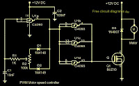
Here is a simple PWM motor speed controller circuit that can be used for varying the speed of low power DC motors .The variation in speed is achieved by varying the duty cycle of the pulse supplied to drive the motor.Of the two gates of IC CD40106B ,N1 is wired as an inverting Schmitt Trigger astable multi vibrator for producing pulses and N2 as an inverting buffer to drive the transistor during positive cycles at base.The duty cycle is set from resistor R2. R1 limits the base current of transistor SL 100.The circuit is ideal for controlling toy motors,hand held mini fans , small blowers etc.
readmore...

Sunday, May 5, 2013

Simple Siren Circuit

This circuit will generate siren sound when S1 pressed and increate sound frequency becuase capacitor C1 charged when switch S1 released the frequency will decreated(C1 discharged).

Try to change resistor R3 if you need to change time interval from low to high frequency and vise versa.
readmore...

Saturday, April 13, 2013

Model Railway Short Circuit Beeper

Short circuits in the tracks, points or wiring are almost inevitable when building or operating a model railway. Although transformers for model systems must be protected against short circuits by built-in bimetallic switches, the response time of such switches is so long that is not possible to immediately localise a short that occurs while the trains are running, for example. Furthermore, bimetallic protection switches do not always work properly when the voltage applied to the track circuit is relatively low. 

Circuit diagram :
Model Railway Short-Circuit Beeper-Circuit Diagram
Model Railway Short-Circuit Beeper Circuit Diagram

The rapid-acting acoustic short-circuit detector described here eliminates these problems. However, it requires its own power source, which is implemented here in the form of a GoldCap storage capacitor with a capacity of 0.1 to 1 F. A commonly available reed switch (filled with an inert gas) is used for the current sensor, but in this case it is actuated by a solenoid instead of a permanent magnet. An adequate coil is provided by several turns of 0.8–1 mm enamelled copper wire wound around a drill bit or yarn spool and then slipped over the glass tube of the reed switch. This technique generates only a negligible voltage drop. The actuation sensitivity of the switch (expressed in ampèreturns or A-t)) deter-mines the number of turns required for the coil. For instance, if you select a type rated at 20–40 A-t and assume a maxi-mum allowable operating current of 6 A, seven turns (40 ÷ 6 = 6.67) will be sufficient. As a rule, the optimum number of windings must be determined empirically, due to a lack of specification data. 

As you can see from the circuit diagram, the short-circuit detector is equally suitable for AC and DC railways. With Märklin transformers (HO and I), the track and lighting circuits can be sensed together, since both circuits are powered from a single secondary winding. 

Coil L1 is located in the common ground lead (‘O’ terminal), so the piezoelectric buzzer will sound if a short circuit is present in either of the two circuits. The (positive) trigger voltage is taken from the lighting circuit (L) via D1 and series resistor R1. Even though the current flowing through winding L1 is an AC or pulsating DC current, which causes the contact reeds to vibrate in synchronisation with the mains frequency, the buzzer will be activated because a brief positive pulse is all that is required to trigger thyristor Th1. The thyristor takes its anode voltage from the GoldCap storage capacitor (C2), which is charged via C2 and R2.  The alarm can be manually switched off using switch S1, since although the thyris-tor will return to the blocking state after C2 has been discharged if a short circuit is present the lighting circuit, this will not happen if there is a short circuit in the track circuit. C1 eliminates any noise pulses that may be generated. 

As a continuous tone does not attract as much attention as an intermittent beep, an intermittent piezoelectric generator is preferable. As almost no current flows during the intervals between beeps and the hold current through the thyristor must be kept above 3 mA, a resistor with a value of 1.5–1.8 kΩ is connected in parallel with the buzzer. This may also be necessary with certain types of continuous-tone buzzers if the operating current is less than 3 mA. The Zener diode must limit the operating voltage to 5.1 V, since the rated volt-age of the GoldCap capacitor is 5.5 V.


source by : Streampowers
readmore...

Thursday, April 11, 2013

Multitasking Pins Circuit

It’s entirely logical that low-cost miniature microcontrollers have fewer ‘legs’ than their bigger brothers and sisters – sometimes too few. The author has given some consideration to how to economise on pins, making them do the work of several. It occurred that one could exploit the high impedance feature of a tri-state output. In this way the signal produced by the high impedance state could be used for example as a CS signal of two ICs or else as a RD/ WR signal. 

Circuit diagram:
multitasking pins circuit diagram Multitasking Pins Circuit Diagram

All we need are two op-amps or comparators sharing a single operating voltage of 5 V and outputs capable of reaching full Low and High levels in 5-V operation (preferably types with rail-to-rail outputs). Suitable examples to use are the LM393 or LM311.The resistances in the voltage dividers in this circuit are uniformly 10 kilo ohms. Consequently input A lies at half the operating voltage (2.5 V), assuming nothing is connected to the input – or the microcontroller pin connected is at high impedance. 

The non-inverting input of IC1A lies at two thirds and the inverting input of IC1B at one third of the operating voltage, so that in both cases the outputs are set at High state. If the microcontroller pin at input A becomes Low, the output of IC1B becomes Low and that of IC1A goes High. If A is High, everything is reversed.


source by :streampowers
readmore...

Simple Mini Audio Amplifier circuit

Description

Here is a simple and humble 2 Watts mini audio amplifier circuit suitable for small pocket radios and other portable audio gadgets.The circuit is based on Phillips Semiconductors IC TDA 7052.The amplifier can be run even from a 3V Mercury button cell.This makes it ideal for battery operated gadgets.

The IC TDA7052 is a mono output amplifier coming in a 8-lead DI package (DIP). The device is mainly designed for battery-operated portable audio circuits. The features of TDA 7052 include ,no external components needed,  no switch-on or switch-off click sounds , great overall stability ,very low power consumption(quiescent current 4mA) , low THD, no  heat sinks required and short-circuit proof.

The gain of TDA 7052 is fixed internally at 40 dB. . To compensate the reduction of output power due to low voltage supply  the TDA7052 uses the Bridge-Tied-Load principle (BTL) which can provide  an output  of around 1 to 2 W  Rms(THD = 10%) into an 8 Ohm load with a power supply of 6 V.

In the circuit the potentiometer can be used to control the volume. Capacitor C1 and C2 are meant for  filtering the supply voltage if a battery eliminator is used as supply source. For operations using a battery C1 and C2 are not necessary.

Mini Audio Amplifier Circuit Diagram with Parts List:

mall Audio Amplifier Circuit

Notes.

  • Assemble the circuit on a good quality PCB or common board .
  • If you are a little expert, you can assemble the  circuit in a match box including the speaker.
readmore...

Wednesday, April 10, 2013

Simple VGA to BNC Adapter Converter Circuit

There are monitors which only have three BNC inputs and which use composite synchronization (‘sync on green’). This circuit has been designed with these types of monitor in mind. As can be seen, the circuit has been kept very simple, but it still gives a reasonable performance. The principle of operation is very straightforward. The RGB signals from the VGA connector are fed to three BNC connectors via AC-coupling capacitors. These have been added to stop any direct current from entering the VGA card. A pull-up resistor on the green output provides a DC offset, while a transistor (a BS170 MOSFET) can switch this output to ground. It is possible to get synchronisation problems when the display is extremely bright, with a maximum green component.

In this case the value of R2 should be reduced a little, but this has the side effect that the brightness noticeably decreases and the load on the graphics card increases. To keep the colour balance the same, the resistors for the other two colors (R1 en R3) have to be changed to the same value as R2. An EXOR gate from IC1 (74HC86) combines the separate V-sync and H-sync signals into a composite sync signal. Since the sync in DOS-modes is often inverted compared to the modes commonly used by Windows, the output of IC1a is inverted by IC1b. JP1 can then by used to select the correct operating mode. This jumper can be replaced by a small two-way switch, if required.

VGA-to-BNC Adapter_165 VGA-to-BNC Adapter diagram_165
   parts VGA-to-BNC Adapter_165pcb VGA-to-BNC Adapter_165

This switch should be mounted directly onto the PCB, as any connecting wires will cause a lot of interference. The PCB has been kept as compact as possible, so the circuit can be mounted in a small metal (earthed!) enclosure. With a monitor connected the current consumption will be in the region of 30 mA. A 78L05 voltage regulator provides a stable 5 V, making it possible to use any type of mains adapter, as long as it supplies at least 9 V. Diode D2 provides protection against a reverse polarity.

LED D1 indicates when the supply is present. The circuit should be powered up before connecting it to an active VGA output, as otherwise the sync signals will feed the circuit via the internal protection diodes of IC1, which can be noticed by a dimly lit LED. This is something best avoided.
Resistors:
R1,R2,R3 = 470Ω
R4 = 100Ω
R5 = 3kΩ3
Capacitors:
C1,C3,C5 = 47µF 25V radial
C2,C4,C6,C7,C10 = 100nF ceramic
C8 = 4µF7 63V radial
C9 = 100µF 25V radial
Semiconductors:
D1 = LED, high-efficiency
D2 = 1N4002
T1 = BS170
IC1 = 74HC86
IC2 = 78L05
Miscellaneous:
JP1 = 3-way pinheader with jumper
K1 = 15-way VGA socket (female), PCB mount (angled pins)
K2,K3,K4 = BNC socket (female), PCB mount, 75Ω    . Link
readmore...